- 您现在的位置:买卖IC网 > Sheet目录3841 > PIC16F737-I/SP (Microchip Technology)IC PIC MCU FLASH 4KX14 28DIP
PIC16F7X7
DS30498C-page 18
2004 Microchip Technology Inc.
2.2.2
SPECIAL FUNCTION REGISTERS
The Special Function Registers are registers used by
the CPU and peripheral modules for controlling the
desired operation of the device. These registers are
implemented as static RAM. A list of these registers is
given in Table 2-1.
The Special Function Registers can be classified into
two sets: core (CPU) and peripheral. Those registers
associated with the core functions are described in
detail in this section. Those related to the operation of
the peripheral features are described in detail in the
peripheral feature section.
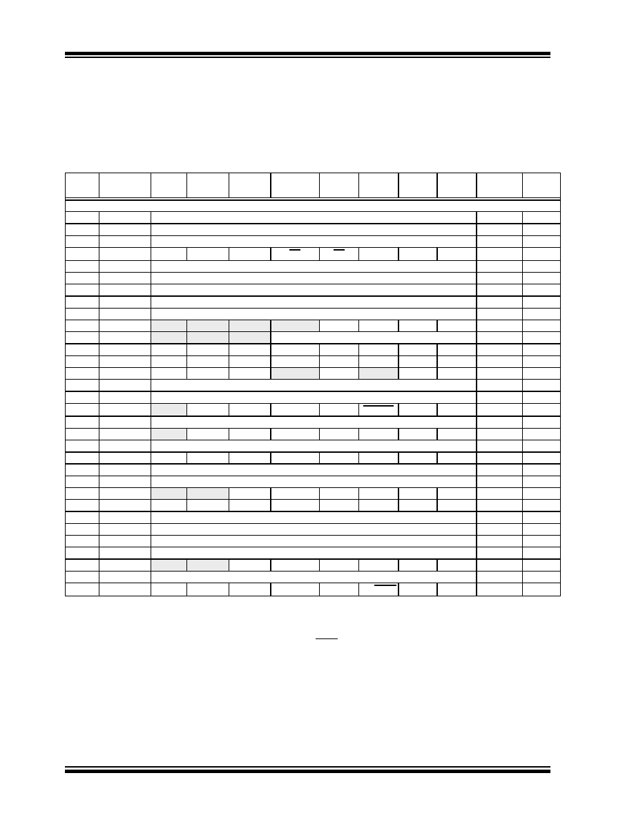
TABLE 2-1:
SPECIAL FUNCTION REGISTER SUMMARY
Address
Name
Bit 7
Bit 6
Bit 5
Bit 4
Bit 3
Bit 2
Bit 1
Bit 0
Value on:
POR, BOR
Details
on page
Bank 0
00h(4)
INDF
Addressing this location uses contents of FSR to address data memory (not a physical register) 0000 0000
01h
TMR0
Timer0 Module Register
xxxx xxxx
02h(4)
PCL
Program Counter (PC) Least Significant Byte
0000 0000
03h(4)
STATUS
IRP
RP1
RP0
TO
PD
ZDC
C
0001 1xxx
04h(4)
FSR
Indirect Data Memory Address Pointer
xxxx xxxx
05h
PORTA
PORTA Data Latch when written: PORTA pins when read
xx0x 0000
06h
PORTB
PORTB Data Latch when written: PORTB pins when read
xx00 0000
07h
PORTC
PORTC Data Latch when written: PORTC pins when read
xxxx xxxx
08h(5)
PORTD
PORTD Data Latch when written: PORTD pins when read
xxxx xxxx
09h(5)
PORTE
—
RE3
RE2
RE1
RE0
---- x000
0Ah(1,4)
PCLATH
—
Write Buffer for the upper 5 bits of the Program Counter
---0 0000
0Bh(4)
INTCON
GIE
PEIE
TMR0IE
INT0IE
RBIE
TMR0IF
INT0IF
RBIF
0000 000x
0Ch
PIR1
PSPIF(3)
ADIF
RCIF
TXIF
SSPIF
CCP1IF
TMR2IF
TMR1IF
0000 0000
0Dh
PIR2
OSFIF
CMIF
LVDIF
—BCLIF
—
CCP3IF
CCP2IF
000- 0-00
0Eh
TMR1L
Holding Register for the Least Significant Byte of the 16-bit TMR1 Register
xxxx xxxx
0Fh
TMR1H
Holding Register for the Most Significant Byte of the 16-bit TMR1 Register
xxxx xxxx
10h
T1CON
—
T1RUN
T1CKPS1
T1CKPS0
T1OSCEN T1SYNC
TMR1CS TMR1ON -000 0000
11h
TMR2
Timer2 Module Register
0000 0000
12h
T2CON
—
TOUTPS3 TOUTPS2
TOUTPS1
TOUTPS0 TMR2ON T2CKPS1 T2CKPS0 -000 0000
13h
SSPBUF
Synchronous Serial Port Receive Buffer/Transmit Register
xxxx xxxx
14h
SSPCON
WCOL
SSPOV
SSPEN
CKP
SSPM3
SSPM2
SSPM1
SSPM0
0000 0000
15h
CCPR1L
Capture/Compare/PWM Register 1 (LSB)
xxxx xxxx
16h
CCPR1H
Capture/Compare/PWM Register 1 (MSB)
xxxx xxxx
17h
CCP1CON
—
CCP1X
CCP1Y
CCP1M3
CCP1M2
CCP1M1
CCP1M0 --00 0000
18h
RCSTA
SPEN
RX9
SREN
CREN
ADDEN
FERR
OERR
RX9D
0000 000x
19h
TXREG
AUSART Transmit Data Register
0000 0000
1Ah
RCREG
AUSART Receive Data Register
0000 0000
1Bh
CCPR2L
Capture/Compare/PWM Register 2 (LSB)
xxxx xxxx
1Ch
CCPR2H
Capture/Compare/PWM Register 2 (MSB)
xxxx xxxx
1Dh
CCP2CON
—
CCP2X
CCP2Y
CCP2M3
CCP2M2
CCP2M1
CCP2M0 --00 0000
1Eh
ADRESH
A/D Result Register High Byte
xxxx xxxx
1Fh
ADCON0
ADCS1
ADCS0
CHS2
CHS1
CHS0
GO/DONE
CHS3
ADON
0000 0000
Legend:
x
= unknown, u = unchanged, q = value depends on condition, — = unimplemented, read as ‘0’, r = reserved.
Shaded locations are unimplemented, read as ‘0’.
Note 1:
The upper byte of the program counter is not directly accessible. PCLATH is a holding register for the PC<12:8> bits, whose contents
are transferred to the upper byte of the program counter during branches (CALL or GOTO).
2:
Other (non Power-up) Resets include external Reset through MCLR and Watchdog Timer Reset.
3:
Bits PSPIE and PSPIF are reserved on the 28-pin devices; always maintain these bits clear.
4:
These registers can be addressed from any bank.
5:
PORTD, PORTE, TRISD and TRISE are not physically implemented on the 28-pin devices (except for RE3), read as ‘0’.
6:
This bit always reads as a ‘1’.
7:
OSCCON<OSTS> bit resets to ‘0’ with dual-speed start-up and LP, HS or HS-PLL selected as the oscillator.
8:
RE3 is an input only. The state of the TRISE3 bit has no effect and will always read ‘1’.
发布紧急采购,3分钟左右您将得到回复。
相关PDF资料
PIC18F86K22-I/PTRSL
MCU PIC 64K FLASH XLP 80TQFP
PIC16C63A-04I/SP
IC MCU OTP 4KX14 PWM 28DIP
PIC16C63A-04I/SO
IC MCU OTP 4KX14 PWM 28SOIC
52559-2270
CONN FFC 22POS .5MM VERT ZIF SMD
52559-1870
CONN FFC 18POS .5MM VERT ZIF SMD
DSPIC33EP64MC506-I/PT
IC DSC 16BIT 64KB FLASH 64TQFP
52745-1896
CONN FFC 18POS .5MM R/A ZIF SMD
PIC16LC622-04/P
IC MCU OTP 2KX14 COMP 18DIP
相关代理商/技术参数
PIC16F737-I/SP
制造商:Microchip Technology Inc 功能描述:IC 8BIT FLASH MCU 16F737 SDIL28
PIC16F737-I/SS
功能描述:8位微控制器 -MCU 7KB 368 RAM 25 I/O RoHS:否 制造商:Silicon Labs 核心:8051 处理器系列:C8051F39x 数据总线宽度:8 bit 最大时钟频率:50 MHz 程序存储器大小:16 KB 数据 RAM 大小:1 KB 片上 ADC:Yes 工作电源电压:1.8 V to 3.6 V 工作温度范围:- 40 C to + 105 C 封装 / 箱体:QFN-20 安装风格:SMD/SMT
PIC16F737T-I/ML
功能描述:8位微控制器 -MCU 7KB 368 RAM 25 I/O RoHS:否 制造商:Silicon Labs 核心:8051 处理器系列:C8051F39x 数据总线宽度:8 bit 最大时钟频率:50 MHz 程序存储器大小:16 KB 数据 RAM 大小:1 KB 片上 ADC:Yes 工作电源电压:1.8 V to 3.6 V 工作温度范围:- 40 C to + 105 C 封装 / 箱体:QFN-20 安装风格:SMD/SMT
PIC16F737T-I/SO
功能描述:8位微控制器 -MCU 7KB 368 RAM 25 I/O RoHS:否 制造商:Silicon Labs 核心:8051 处理器系列:C8051F39x 数据总线宽度:8 bit 最大时钟频率:50 MHz 程序存储器大小:16 KB 数据 RAM 大小:1 KB 片上 ADC:Yes 工作电源电压:1.8 V to 3.6 V 工作温度范围:- 40 C to + 105 C 封装 / 箱体:QFN-20 安装风格:SMD/SMT
PIC16F737T-I/SS
功能描述:8位微控制器 -MCU 7KB 368 RAM 25 I/O RoHS:否 制造商:Silicon Labs 核心:8051 处理器系列:C8051F39x 数据总线宽度:8 bit 最大时钟频率:50 MHz 程序存储器大小:16 KB 数据 RAM 大小:1 KB 片上 ADC:Yes 工作电源电压:1.8 V to 3.6 V 工作温度范围:- 40 C to + 105 C 封装 / 箱体:QFN-20 安装风格:SMD/SMT
PIC16F73-E/ML
功能描述:8位微控制器 -MCU 7 KB 368 RAM 25I/O RoHS:否 制造商:Silicon Labs 核心:8051 处理器系列:C8051F39x 数据总线宽度:8 bit 最大时钟频率:50 MHz 程序存储器大小:16 KB 数据 RAM 大小:1 KB 片上 ADC:Yes 工作电源电压:1.8 V to 3.6 V 工作温度范围:- 40 C to + 105 C 封装 / 箱体:QFN-20 安装风格:SMD/SMT
PIC16F73-E/SO
功能描述:8位微控制器 -MCU 7KB 192 RAM 22 I/O RoHS:否 制造商:Silicon Labs 核心:8051 处理器系列:C8051F39x 数据总线宽度:8 bit 最大时钟频率:50 MHz 程序存储器大小:16 KB 数据 RAM 大小:1 KB 片上 ADC:Yes 工作电源电压:1.8 V to 3.6 V 工作温度范围:- 40 C to + 105 C 封装 / 箱体:QFN-20 安装风格:SMD/SMT
PIC16F73-E/SP
功能描述:8位微控制器 -MCU 7KB 192 RAM 22 I/O RoHS:否 制造商:Silicon Labs 核心:8051 处理器系列:C8051F39x 数据总线宽度:8 bit 最大时钟频率:50 MHz 程序存储器大小:16 KB 数据 RAM 大小:1 KB 片上 ADC:Yes 工作电源电压:1.8 V to 3.6 V 工作温度范围:- 40 C to + 105 C 封装 / 箱体:QFN-20 安装风格:SMD/SMT